Memory mapped I/O
In order to study exceptions and interrupts we will use the Mips 32 simulator Mars. All instructions will be written for and tested using Mars but you should be able to use the Spim simulator if you prefer.
Mips system architecture
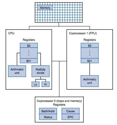
A Mips processor consists of an integer processing unit (the CPU) and a collection of coprocessors that perform ancillary tasks or operate on other types of data such as floating-point numbers.
Both Mars and Spim simulates two coprocessors:
- Coprocessor 0 handles exceptions and interrupts.
- Coprocessor 1 is the floating-point unit.
Integer arithmetic and logical operations are executed directly by the CPU. Floating point operations are executed by Coprocessor 1. Coprocessor 0 are used do manage exceptions and interrupts.
Receiver and transmitter
Mars simulates one I/O device: a memory-mapped console on which a program can read and write characters. The terminal device consists of two independent units: a receiver and a transmitter.
- The receiver reads characters typed on the keyboard.
- The transmitter display characters on the console.
Echo
The receiver and transmitter are completely independent. This means, for example, that characters typed at the keyboard are not automatically echoed on the display. Instead, a program must explicit echo a character by reading it from the receiver and writing it to the transmitter.
Memory layout
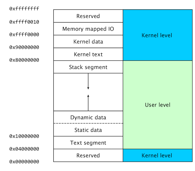
To execute a Mips program memory must be allocated. The Mips computer can
address 4 Gbyte of memory, from address 0x0000 0000 to 0xffff ffff. User memory
is limited to locations below 0x7fff ffff. In the below figure the layout of the
memory allocated to a Mips program is shown.
The purpose of the various memory segments:
- The user level code is stored in the text segment.
- Static data (data know at compile time) use by the user program is stored in the data segment.
- Dynamic data (data allocated during runtime) by the user program is stored in the heap.
- The stack is used by the user program to store temporary data during for example subroutine calls.
- Kernel level code (exception and interrupt handlers) are stored in the kernel text segment.
- Static data used by the kernel is stored in the kernel data segment.
- Memory mapped registers for IO devices are stored in the memory mapped IO segment.
Memory-mapped terminal device
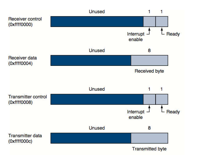
A program controls the terminal with four memory-mapped device registers. Memory-mapped means that each register appears as a special memory location. In this sense, these are not real registers but simply words (32 bit) values stored in memory.
Receiver control
The Receiver Control register is at memory location 0xffff0000. Only two of its
bits are actually used.
Bit 0 is called ready:
- If it is 1, it means that a character has arrived from the keyboard but has not yet been read from the Receiver Data register.
- The ready bit is read-only: writes to it are ignored.
- The ready bit changes from 0 to 1 when a character is typed at the key- board, and it changes from 1 to 0 when the character is read from the Receiver Data register.
Bit 1 is the keyboard interrupt enable bit:
- This bit may be both read and written by a program.
- The interrupt enable is initially 0.
- If it is set to 1 by a program, the terminal requests an interrupt at hardware level 1 whenever a character is typed and the ready bit becomes 1. However, for the interrupt to affect the processor, interrupts must also be enabled in the Status register.
- All other bits of the Receiver Control register are unused.
Receiver data
The second terminal device register is the Receiver Data register at memory
address 0xffff0004.
- The low-order 8 bits of this register contain the last character typed at the keyboard. All other bits contain 0s.
- This register is read-only and changes only when a new character is typed at the keyboard.
- Reading the Receiver Data register resets the ready bit in the Receiver Control register to 0.
- The value in this register is undefined if the Receiver Control register is 0.
Transmitter control
The third terminal device register is the Transmitter Control register at memory
address 0xffff0008. Only the low-order 2 bits of this register are used. They
behave much like the corresponding bits of the Receiver Control register.
Bit 0 is called ready:
- This bit is read-only.
- If this bit is 1, the transmitter is ready to accept a new character for output.
- If it is 0, the transmitter is still busy writing the previous character.
Bit 1 is the interrupt enable bit:
- This bit is readable and writable.
- If this bit is set to 1, then the terminal requests an interrupt at hardware level 0 whenever the transmitter is ready for a new character and the ready bit becomes 1.
Transmitter data
The final device register is the Transmitter Data register at memory address
0xffff000c.
Only the least 8 significant bits (the least significant byte) are used:
- When a value is written into this location, its low-order 8 bits (i.e., an ASCII character) are sent to the console.
- When the Transmitter Data register is written, the ready bit in the Transmitter Control register is reset to 0. This bit stays 0 until enough time has elapsed to transmit the character to the terminal; then the ready bit becomes 1 again.
- The Transmitter Data register should only be written when the ready bit of the Transmitter Control register is 1. If the transmitter is not ready, writes to the Transmitter Data register are ignored (the write appears to succeed but the character is not output).
Timing
In a physical computer sending a character to the terminal doesn’t happen instantly, the operation takes some time to complete.
The simulators Mars and SPIM measures time by counting the number executed instructions , not in real clock time. After writing a character to the receiver data register, this means that the transmitter does not become ready again until the processor executes a fixed number of instructions. If you stop the simulation and look at the ready bit, it will not change. However, if you let the simulation continue, the bit eventually changes back to 1.


